


 22-23 / 568

Eco-Friendly metallic Coatings for printed parts
(metal).
Barak Noy
Advisor: Professor Adin Stern
Mechanical Engineering
Abstract
In the current study, a simple to use environmentally friendly electroless Au-Ag plating was
developed and applied on top of AM-LPBF AlSi10Mg specimens in order to improve the surface
appearance based on aesthetics considerations. There was a necessity to develop a special
electroless process suitable for the cover of 3D-printed AlSi10Mg. The results displayed good-
quality and satisfactory shiny appearance Au-Ag coating surfaces for both processes
temperatures .The current developed electroless Au-Ag coating process can be adapted for
various applications, including 3D printed items for museum exhibitions.
Coating Process
Summary
•
Additive manufacturing (AM) is defined as manufacturing processes developed for joining
preferred materials by printing layer upon layer from 3D objects. Selective Laser Melting
(SLM) is rapid AM technology uses a high power density laser to melt and join metallic
powder. In some AM-SLM parts, additional coating is needed for: electrical conductivity
enhancement, or matching decoration considerations.
•
There is increase of about 22% ± 2% of the “real” surface area compared with the “ideal”
surface.
•
The Electrum coating process on
AlSi10Mg
models accomplished successfully.
•
The Electrum coating thickness is between 0.8-2.6μm.
•
Roughness values measured approximately 15 μm Ra.
•
Generally roughness values decreasing with coating thickness.
Samples
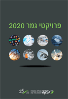
The AM-LPBF AlSi10Mg disk-shaped specimens (26 mm in diameter) were built in the vertical
Z direction (Fig. >), with the circular surface perpendicular to the build-platform. The printed
specimens were heat-treated at 300
o
C for 2 h and then cooled in still air. The specimens
contain obverse side with two steps, simulating the roughness of ancient coins (each step
height is 1 mm), and a planar surface on the reverse (back) side.
Samples under 3D microscope before and after plating
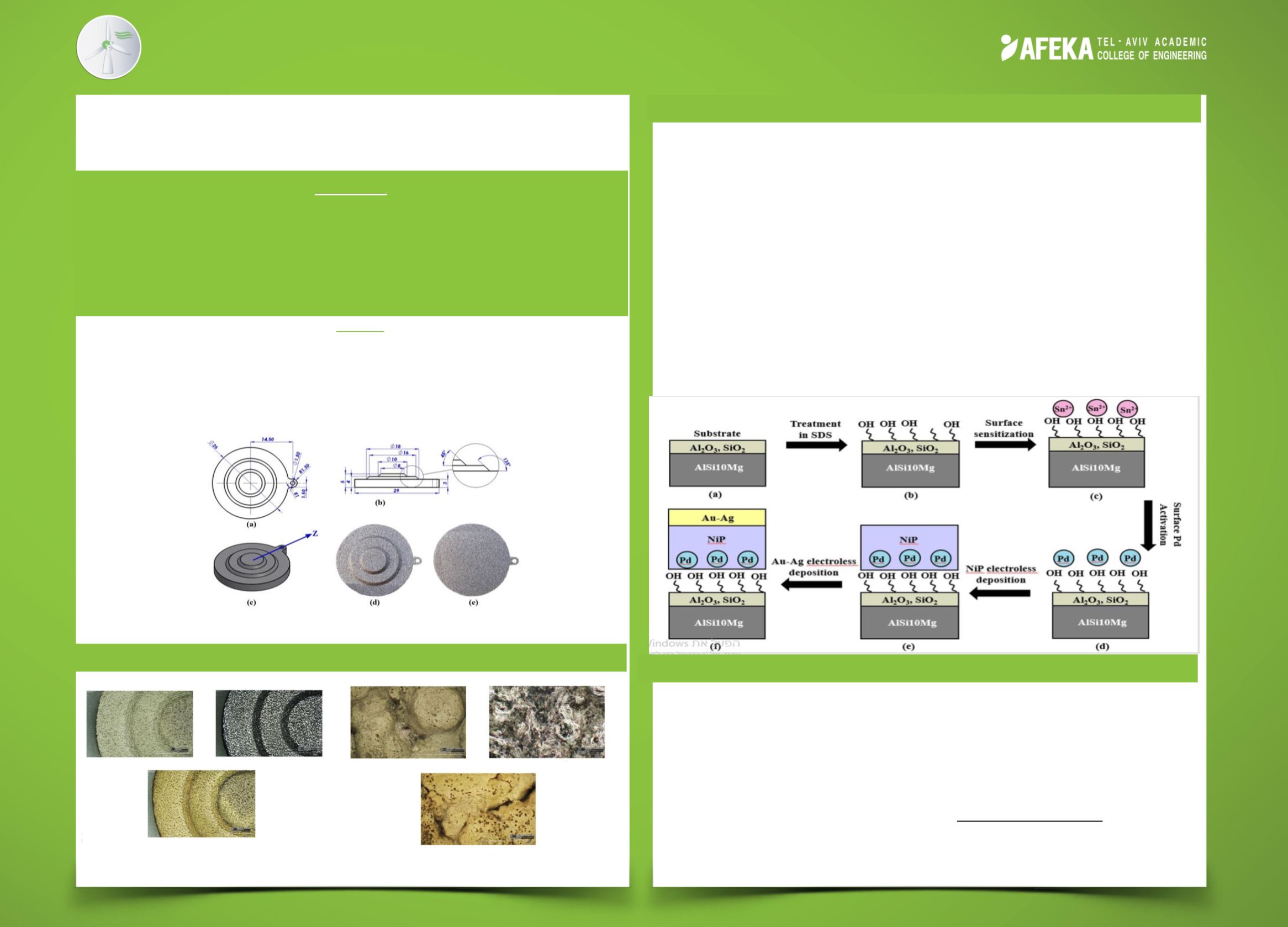
An electroless Au-Ag plating process was developed in the present study (Fig.3&2 >). Prior
to the deposition process, the surface of all AlSi10Mg specimens was cleaned and etched in
12 g/l SDS (sodium dodecyl sulphate) solution at room temperature for 10 min in ultrasonic
bath (Fig. >b). The quality of the coating is intensely dependent on both the pretreatment of
the printed substrates and the cleaning process. The cleaning process reduced the weight of
the AlSi10Mg specimens by 0.001 g. Next a sensitization process was applied in SnCl
2
/HCl
(70 g/l of SnCl
2
and 40 ml/l of HCl) solution at room temperature for 2 min (Fig. >c). Surface
palladium activation was performed in Pd-citrate solution (0.1 g/l of PdCl
2
, 7.35 g/l of citric
acid, 2.8 g/l of NaOH and 2.4 g/l of HCl) at room temperature for 1 min (Fig. >d). This step is
applied in order to create metal catalytic seeds that serve as nucleation sites. A NiP
interlayer was electroless deposited (Fig. >e) on the specimens to improve an adhesion of
the alloy to the substrate. Only then the electroless electrum (Au-Ag) plating was finally
performed (Fig. >f) at two temperatures (80 and 90
o
C) and time intervals of 1.5 to 9
minutes. The 3D-printed specimens were washed after each step and at the end of the Au-
Ag deposition process in DI water. Following the electrum deposition, the Au-Ag coated
specimens were heated in an air oven at 100
o
C for 30-60 min.
Fig. 1 disk-shaped specimens
Fig. 3 specimens X600: S7 (top right)
without coating, S23 (top left),S25
(bottom)
Fig. 2 specimens X20: S7 (top right)
without coating, S23 (top left) ,S25
(bottom)