


 318-319 / 568

Morphological Co-Processing Unit
Project Goals:
1. Implementing morphological image processing on FPGA using HDL.
2. Processing time need to be better than general-purpose CPU.
3. Present the image processing results on the screen using VGA cable and
interface implemented on the FPGA.
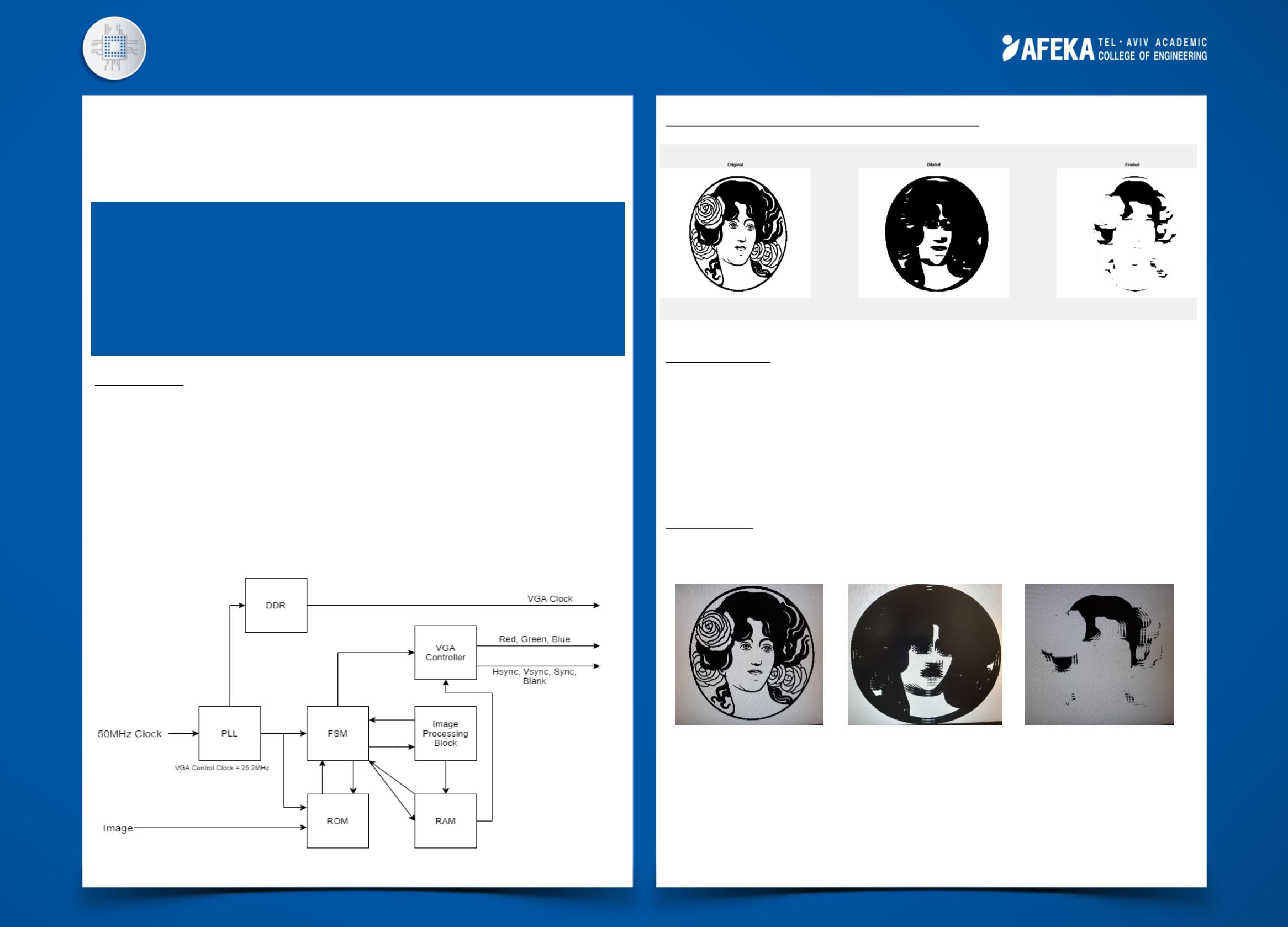
System Structure:
The system is comprised of Altera Cyclone IV chip on DE2 board. The board
connected with VGA cable to LCD screen to present the results.
The main part of the system is the HDL code in the FPGA.
Michael Astahov
Advisor: Dr. Binyamin Abramov
Electrical Engineering
Matlab simulation for the expected FPGA results:
Data Processing:
1. Fetching the data from the FPGA ROM.
2. Send the pixels to the image processing block.
3. Store the results in RAM memory block.
4. Fetching the pixels data from the RAM to the VGA interface block to send the
data to the VGA cable.
FPGA Results:
The result as can be seen from the screen connected with VGA cable:
The FPGA return the results after 0.5msec of processing time, better performance
than general-purpose CPU using programming language.
In a reality of constant demand for ultra-fast data and image
processing like in the vehicular automation, there is a need
for a solution that could perform image processing much
faster than general-purpose CPU. This system perform
morphological image processing using FPGA and present the
results on the screen with VGA interface.
Original
Dilated
Eroded
Original
Dilated
Eroded